Actual Customer Application Case of Screen Printing (PCB Circuit Board Industry)
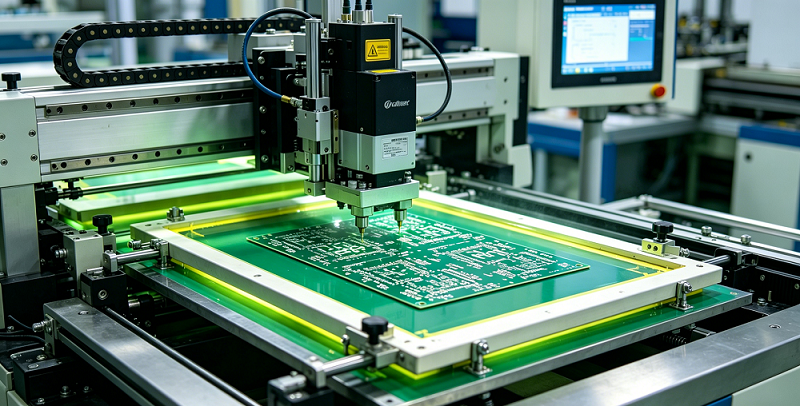
Actual Customer Application Case of Screen Printing (PCB Circuit Board Industry)
I. Basic Customer Information
A professional PCB circuit board manufacturing enterprise (specializing in the R&D and production of rigid PCBs and flexible PCBs, whose products are widely used in consumer electronics, industrial control, automotive electronics and other fields, with an annual output of 1.2 million square meters, serving many well-known domestic and foreign electronic terminal manufacturers).
Customer Needs: To provide screen printing services for rigid PCB circuit boards, mainly used for circuit solder mask and character marking printing. The core needs cover three dimensions: first, high printing precision, with clear solder mask lines without ink overflow, clear and distinguishable character marks (component labels, specification parameters), and dimensional deviation controlled within ±0.05mm; second, qualified performance, with strong solder resistance of the solder mask layer, which can withstand the high temperature of 260℃ reflow soldering, excellent adhesion without bubbling or peeling, and friction-resistant and chemical corrosion-resistant characters; third, production capacity adaptation, which can meet the mass production demand of 3,000 PCB boards per day (specification: 100mm×150mm), the delivery cycle is controlled within 3 days, and the ink must comply with the RoHS environmental protection standard of the electronic industry, without heavy metals or harmful substances.
Customer Pain Points: The previous cooperative printing supplier had three major problems: first, insufficient printing precision of the solder mask layer, which was prone to ink overflow and bridging, leading to short circuits of PCB circuits, with a rework rate as high as 8%; second, poor solder resistance of the solder mask layer, which was prone to bubbling and peeling after reflow soldering, affecting product qualification rate; third, blurred and easy-to-peel character printing, making it impossible to clearly identify component labels during subsequent inspection, increasing manual sorting costs, and unstable delivery cycles affecting the PCB assembly progress.

II. Cooperation Background and Demand Analysis
To expand the markets of automotive electronics and industrial control, the PCB manufacturing enterprise launched high-precision rigid PCB circuit board products. Such products have much higher requirements on the precision and performance of solder mask and character printing than ordinary consumer electronic PCBs, requiring supporting high-quality screen printing services, which not only meet the strict standards of the electronic industry, but also take into account the stability and efficiency of mass production. Combined with the customer's product characteristics, we accurately analyzed its needs:
-
Substrate Adaptation: The printing substrate is FR-4 rigid PCB substrate (copper cladding thickness 1oz-2oz), whose surface has been roughened. It is necessary to solve the adhesion problem between solder mask ink, character ink and the substrate and copper foil to avoid falling off in high temperature and chemical environments;
-
Performance Requirements: The solder mask ink must have high temperature resistance (260℃ reflow soldering, no abnormality after 10 seconds of heat preservation), chemical corrosion resistance (can withstand immersion in flux and cleaning agent), excellent insulation performance (breakdown voltage ≥10kV/mm), and adhesion ≥3.0N/25mm; the character ink must be friction-resistant (friction resistance ≥1000 times), alcohol-wipe resistant (no peeling after 50 times), and have clear color (black characters with high contrast);
-
Precision Requirements: The deviation of the solder mask window opening size is ≤±0.05mm, without ink overflow or bridging, and the line spacing is ≥0.1mm; the character line width is ≤0.15mm, clear without burrs, the character position deviation is ≤±0.1mm, and it can be identified by AOI automatic detection;
-
Production Capacity and Delivery: The daily output is ≥3,000 PCB boards, the delivery cycle of regular orders is ≤3 days, and urgent orders can be responded to within 12 hours, adapting to the whole process rhythm of the customer's PCB substrate production and welding assembly, and the rework rate is controlled within 1%.
III. Design and Implementation of Screen Printing Solution
Combined with the customer's needs and pain points, we set up a special technical team for PCB screen printing, and formulated a customized solution of "substrate pre-treatment + high-precision screen production + automatic printing + layered curing + full-process quality inspection". Relying on high-precision UV screen printing technology, we focused on the core pain points of solder mask and character printing, and achieved dual improvement in product quality and production efficiency. The specific implementation steps are as follows:
(I) Preparations: Substrate Pre-treatment and Screen Customization
1. Substrate Pre-treatment: For FR-4 PCB substrates, first use alkaline cleaning solution to remove surface oxide layers, oil stains and impurities, then perform micro-etching treatment (micro-etching depth 0.5-1.0μm) to improve the surface roughness of the substrate and enhance ink adhesion; after pre-treatment, use high-pressure air knife to dry, ensuring that the substrate surface is clean, free of moisture and residues, and the cleanliness reaches Class 100 standard, laying the foundation for subsequent printing.
2. Screen Customization: According to the PCB printing precision requirements, 600-mesh to 800-mesh stainless steel screens are selected (800-mesh for solder mask printing and 600-mesh for character printing). The photosensitive adhesive is high-resolution solvent-resistant photosensitive adhesive, with a thickness controlled at 8-12μm, the screen tension maintained at 30-35N/cm, and the tension uniformity deviation ≤2%; after the screen pattern is confirmed by the customer's PCB Gerber file, it is produced by Laser Direct Imaging (LDI) technology to accurately restore the solder mask window opening and character pattern, ensuring smooth line edges without burrs and precise positioning marks, providing guarantee for overprinting calibration.
3. Ink Selection: Special PCB ink complying with RoHS environmental protection standards is selected. The solder mask ink is high-temperature resistant epoxy UV curing ink, added with curing accelerator to ensure no bubbling or peeling during 260℃ reflow soldering and qualified insulation performance; the character ink is fast-drying UV black ink, with strong adhesion and high contrast, which can clearly identify component labels, and is alcohol-resistant and friction-resistant; the ink contains no heavy metals such as lead and cadmium, and the VOCs content is ≤20g/L, which fully complies with the environmental protection standards of the electronic industry, and the color completely matches the character standard color required by the customer.
(II) Printing Implementation: Automatic Equipment and Process Optimization
1. Equipment Selection: A special automatic screen printing machine for PCB is adopted, equipped with a high-precision visual positioning system (10-megapixel camera), which can automatically identify the reference points of the PCB substrate to achieve precise positioning with a positioning deviation ≤±0.003mm; it is equipped with a vacuum adsorption platform to ensure the flatness of the PCB substrate and avoid displacement during printing; special printing units are respectively equipped for solder mask and character printing to realize one feeding and two printings (solder mask + character), improving production efficiency and reducing manual operation errors.
2. Process Parameter Optimization: According to the characteristics of PCB substrates and ink performance, the printing parameters are optimized: the scraper is made of tungsten steel with a hardness of 85-90 Shore A, an angle of 70°-80°, a pressure of 20-30N/cm², and a printing speed of 10-15cm/s; after solder mask printing, an LED UV curing machine (wavelength 395nm, power 800W) is used with a curing time of 3-5 seconds to ensure full curing of the solder mask layer and avoid problems in subsequent reflow soldering; after character printing, low-temperature UV curing is adopted (temperature 60℃, curing time 2-3 seconds) to prevent high temperature from damaging the PCB substrate and copper foil, and ensure rapid curing of character ink and improve adhesion.
3. Precise Positioning and Overprinting Control: Before printing, the reference calibration of the PCB substrate is carried out through the visual positioning system. After the solder mask printing is completed, the positioning calibration is performed again to ensure that the character printing is accurately aligned with the solder mask window opening, with a position deviation ≤±0.1mm; during the printing process, the ink viscosity is monitored in real time, maintained at 40-50 seconds (coating cup 4) to ensure uniform ink transfer, the solder mask layer thickness is controlled at 10-15μm, the character layer thickness is controlled at 5-8μm, and the thickness deviation ≤±1μm; an automatic ink overflow detection is set during the printing process to timely reject unqualified products with ink overflow and bridging, reducing the rework rate.

(III) Post-processing and Quality Control
1. Post-processing: After printing, deburring treatment is performed on the PCB board to remove excess ink on the printing edge and ensure no line bridging; high-pressure air gun is used to blow off surface dust to avoid dust affecting subsequent welding; some high-end PCB boards are coated with film to protect the solder mask layer and characters from damage during transportation and storage.
2. Full-process Quality Inspection: A three-level quality inspection system is established. Level 1 Quality Inspection (during printing): sampling inspection is conducted every 20 minutes to check printing precision, ink thickness and ink overflow; Level 2 Quality Inspection (after curing): AOI automatic optical inspection system is used to detect solder mask window opening size, character clarity and position deviation with a detection precision of ±0.005mm, and unqualified products are automatically rejected; Level 3 Quality Inspection (before delivery): adhesion test (cross-cut method), solder resistance test (260℃ reflow soldering with 10 seconds of heat preservation), insulation performance test and alcohol wipe test are carried out to ensure that the products meet customer standards and electronic industry specifications, the qualification rate is maintained above 99.2%, and the rework rate is controlled within 0.8%.
IV. Cooperation Achievements and Customer Feedback
(I) Cooperation Achievements
-
Qualified Quality: The printed products fully meet customer and electronic industry standards, with no ink overflow or bridging in the solder mask layer, the window opening size deviation ≤±0.04mm, excellent solder resistance, no bubbling or peeling after 260℃ reflow soldering, and qualified insulation performance (breakdown voltage ≥12kV/mm); the characters are clear and distinguishable, with smooth lines without burrs, alcohol-wipe resistant and friction-resistant, and can be identified by AOI automatic detection, completely solving the previous quality pain points.
-
Production Capacity Adaptation: The daily output of 3,500 PCB boards is achieved, the delivery cycle of regular orders is shortened to 2.5 days, and urgent orders can be delivered within 12 hours, which fully matches the progress of the customer's PCB substrate production and welding assembly, with no order delay, effectively ensuring the customer's downstream delivery.
-
Cost Optimization: Through automatic production and full-process quality inspection, the rework rate is reduced from 8% to 0.8%, greatly reducing manual rework costs; the improvement of ink adhesion and solder resistance reduces the subsequent product failure maintenance cost by about 30%; the use of environmentally friendly ink helps customers' products pass international certifications such as RoHS and REACH, expanding overseas markets.
-
Long-term Cooperation: With stable product quality, efficient delivery capacity and professional technical support, we have established a long-term strategic cooperative relationship with the customer, becoming the exclusive supplier of solder mask and character printing for its high-precision PCB circuit boards. The cooperation cycle has exceeded 4 years, the annual cooperation volume has increased year by year, and we have synchronously cooperated with the customer to complete the printing process R&D of new products.
(II) Customer Feedback
"This cooperation has completely solved the core pain points of our PCB printing. The precision and solder resistance of the solder mask layer and the clarity of the characters fully meet the requirements of high-precision PCBs. The rework rate has dropped significantly, effectively reducing our production costs. The supplier's technical team responds quickly and can optimize the printing process according to our product upgrade needs. The delivery cycle is stable, providing strong guarantee for our production progress. It is a trustworthy long-term partner, and we look forward to deepening cooperation in the field of flexible PCB printing in the future." ——Person in Charge of Customer Production Department
V. Case Summary
This case focuses on the practical application of screen printing in the PCB circuit board industry. Aiming at the customer's core needs in the precision, solder resistance, production capacity and other aspects of solder mask and character printing, through precise substrate adaptation, high-precision screen production, automatic printing process optimization and full-process quality inspection, it has achieved dual improvement in product quality and production efficiency, solving the pain points of traditional screen printing in the PCB field such as ink overflow, poor solder resistance, blurred characters and unstable delivery.
With the advantages of high precision, strong adhesion and wide adaptability, screen printing plays an irreplaceable role in the field of PCB circuit board solder mask and character printing. Precise demand analysis, customized solutions, strict quality control and efficient delivery capacity are the keys to realizing customer value and establishing long-term cooperation. In the future, we can further combine intelligent production technology to optimize the printing process, improve product precision and production efficiency, adapt to the personalized printing needs of high-end products such as flexible PCBs and high-frequency PCBs, and help customers expand more high-end electronic field markets.
Screen Printing Consumables for Cosmetic Bottle Printing: Applications, Materials, and Industry Advantages
Application Case of Screen Printing Mesh and Frame in Printing